RFID EM Module Potting Process|ODM Customized Embedded RFID Module
Why Potting Is Applied to RFID EM Modules
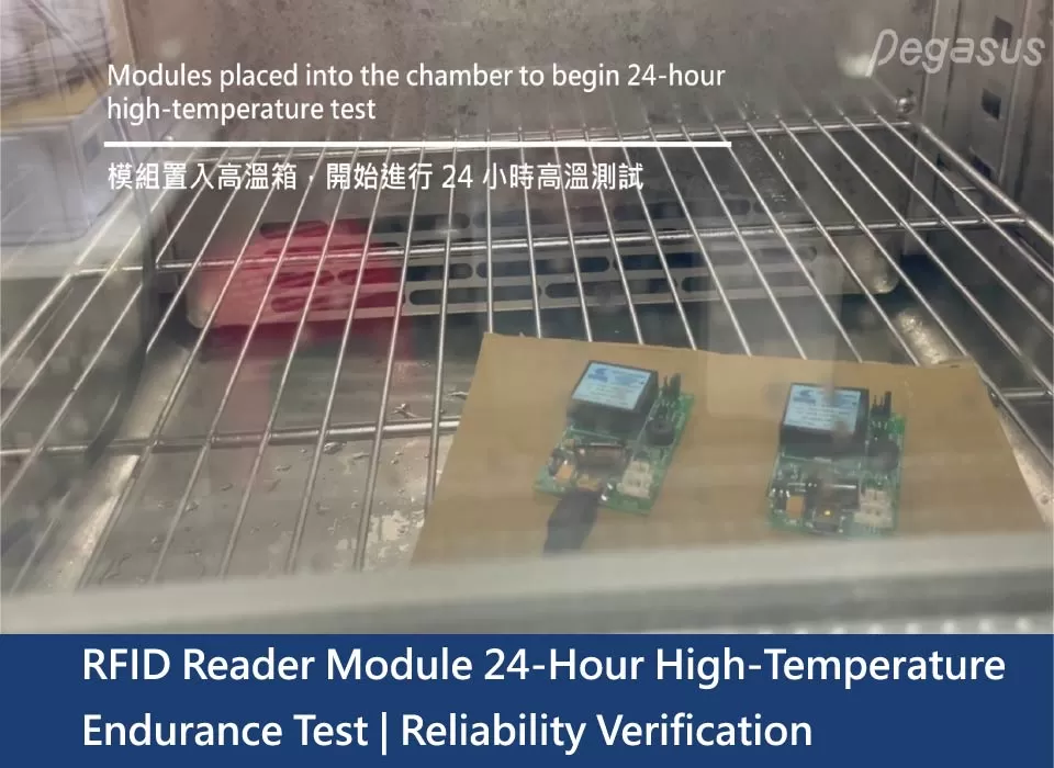
In embedded RFID applications, modules are often required to operate continuously in industrial environments, semi-open spaces, or inside equipment enclosures.
To ensure stable and consistent performance under real-world operating conditions, potting is typically applied after antenna soldering and functional verification, serving as an essential step in the manufacturing process.
Potting is not intended to enhance reading performance, but rather to protect circuit structures, improve long-term reliability, and reduce the impact of environmental factors on electronic components.
Role of the Potting Process in Manufacturing
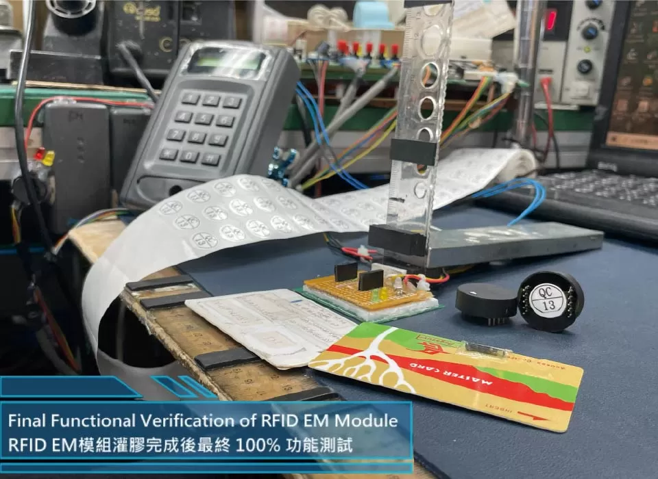
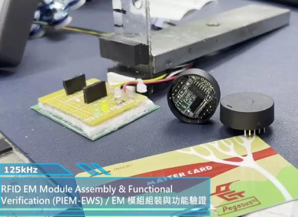
The potting process shown in this video is performed after the following prerequisites are completed:
- Antenna soldering
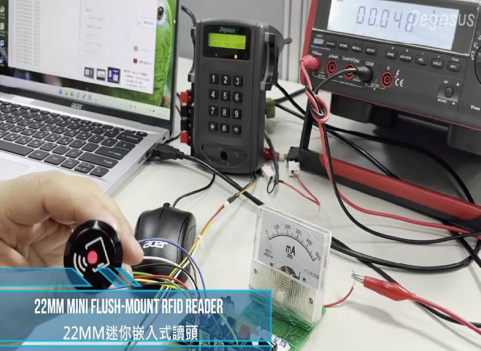
- Functional verification and reading tests
- Confirmation of basic electrical performance
Applying potting at this stage prevents premature encapsulation before functional validation, ensuring process controllability and production consistency.
Manual Potting for ODM Customization
In OEM / ODM projects, customer requirements may vary in terms of module structure, installation method, or operating environment.
For this reason, manual potting is often adopted to allow precise adjustment of potting locations and material volume according to specific specifications.This approach is particularly suitable for:
- Low-volume, high-mix customized production
- Modules designed for different housings or application conditions
- ODM projects requiring manufacturing flexibility and process control
Engineering Objectives of the Potting Process
The primary engineering objectives of the potting process include:
- Protecting circuitry and solder joints
- Reducing mechanical stress caused by vibration or long-term operation
- Enhancing overall module reliability under moisture, dust, or oil-exposed environments
- Serving as part of process standardization to align reliability baselines across different projects
About the Process Demonstration Video
The accompanying video on this page provides a demonstration of the RFID EM module potting process, illustrating the actual manufacturing stage and workflow context.
The video does not represent:- Installation instructions
- Performance or protection level specifications
- Guarantees for specific application scenarios
Engineering Value for OEM / ODM Applications
By clearly separating manufacturing stages such as soldering, verification, potting, and final testing, OEM / ODM projects can achieve improved integration efficiency and quality control, reducing risks during system implementation and long-term operation.